To avoid errors during the PCB assembly process, the following points are essential.
Feb 22, 2024
One. Offer completely PCB fabrication production files to manufacturer
BOM List
Gerber
Pnp file
PCBA testing file
Two. PCB manufacturing and assembly drawing
Specification of PCB bare board:
Drilling a hole
Hole map
The layers are stacked
Notes (PCB material and thickness, copper weight, tolerances,Surface finish, and special requirements)
Circuit Board Assembly Instructions:
Circuit Board Overview
Component Shapes
Bill of Materials
Mechanical Parts
Assembly Instructions
Additional Notes
Expanded Cross-Section View
Identification Tag Locations
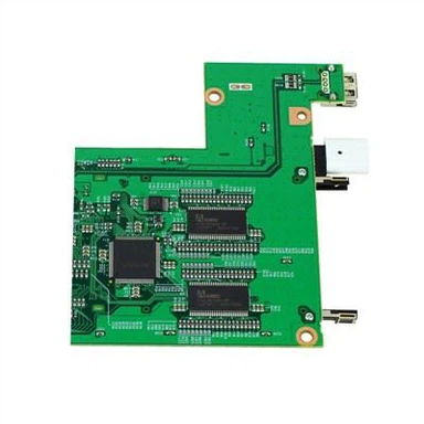
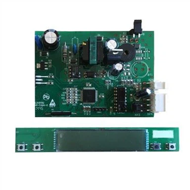
Three. Correct PCB Assembly

Four. Make sure the silkscreen is be clearly visible
Circuit Board Overview
Component Shapes
Bill of Materials
Mechanical Parts
Assembly Instructions
Additional Notes
Expanded Cross-Section View
Identification Tag Locations
Five. Make sure the silkscreen is be clearly visible

Six, Identify the polarity of electronic components
The cathode and anode are identified on components such as electrolytic capacitors, leds, diodes and ics

Seven. Isolate leaded and lead-free electronic components
Seven. Component spacing
Avoid the problem of spacing between components during assembly

Eight. Large components are placed evenly
Large components are placed evenly so that the heat can be evenly distributed during reflow soldering, and the PCBA manufacturer will set the heat curve of reflow soldering.
Nine. DFM Check
Design for Manufacturability (DFM) checks can identify design errors at an early stage and prevent problems such as rework repairs at a later stage